What the 12 ns access time means for your bus
The CY7C1399B-12ZXC is a 256Kbit asynchronous SRAM organized as 32K x 8 bits, with a 12 ns access time that sets the fastest read cycle the CPU can expect without wait states. In a 3.3 V system, that 12 ns window covers address-to-data valid — if your controller's memory bus runs at 50 MHz (20 ns cycle), this part leaves 8 ns of margin for address hold and data setup, which is tight but workable for a single-cycle read.
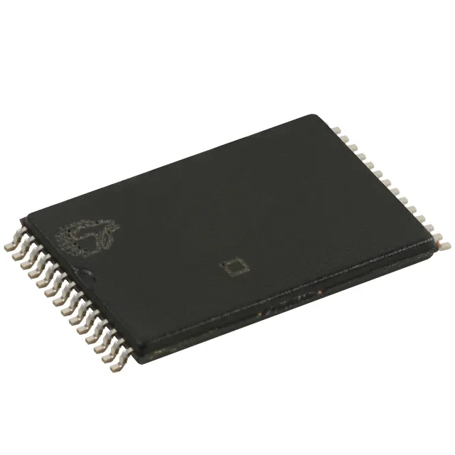
Package and hand-solderability
No BGA, no hidden pads; you can breadboard it on a SOIC adapter if you're prototyping.
The commercial temperature range (0°C to 70°C) limits it to indoor, climate-controlled environments — not suitable for engine bays or outdoor enclosures without active cooling.
Obsolete — sourcing reality
Infineon lists this part as Obsolete. If you're designing a new board, look for a current-generation async SRAM in the same 28-TSOP footprint — the 12 ns speed grade and 3.3 V supply are common across many active parts.