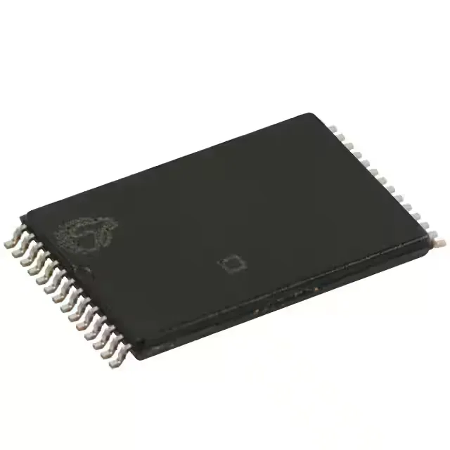
Fast asynchronous SRAM for cache and buffer applications
This part is intended for use as a fast scratchpad, cache tag memory, or data buffer in embedded systems, networking equipment, and test instrumentation where the 12 ns cycle time keeps pace with mid-speed processors and FPGAs without wait states.
The 12 ns access time means the SRAM can complete a read or write cycle in 12 ns, which translates to a maximum bus frequency of roughly 83 MHz for back-to-back accesses. In practice, this allows a 66 MHz or 75 MHz bus to run without inserted wait states, saving logic and keeping memory latency deterministic. The write cycle time matches the read access at 12 ns, so mixed read/write traffic sees no penalty on the write side.
Buyers should plan for last-time-buy quantities or qualify a pin-compatible alternative for new production.
Package and footprint — 28-TSOP I
It is surface-mount and intended for reflow soldering. The shipping medium is tray. The narrow 0.465-inch body is common for 28-pin TSOP I SRAMs, so the footprint is shared with many other 32K x 8 asynchronous SRAMs from Cypress, ISSI, and Alliance Memory, easing second-source qualification.