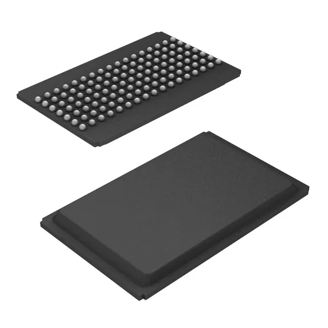
18 Mbit synchronous SRAM for pipelined controllers
The CY7C1372D-167BGC: The x18 data width suits systems that need parity or a wider data path without pairing two x8 parts — common in network switch buffers and DSP memory maps where the extra two bits carry control or ECC metadata. The access time is the spec that determines whether the SRAM can run at zero wait states with a given controller's input setup timing; at 167 MHz the cycle period is 6 ns, so the 3.4 ns access leaves 2.6 ns of margin for the controller's data-hold window.
Infineon lists the CY7C1372D-167BGC as Obsolete. For sustainment programs that require a form-fit-function replacement, a board-level evaluation of alternative synchronous SRAMs in the same 119-BGA footprint is necessary — there is no drop-in pin-compatible second source documented.
119-BGA package and board integration
Housed in a 119-ball PBGA (14x22 mm body) with a 1.27 mm ball pitch, the package is layout-friendly for a 4-layer PCB — no micro-vias or buried vias required for fan-out. The supplier device package is 119-PBGA (14x22). There is no exposed thermal pad; the junction-to-board thermal path relies on the BGA balls and the inner copper planes.
Commercial temperature grade and supply rails
For designs that see extended industrial or automotive ambient temperatures, this part is not rated. The supply voltage range is 3.135 V to 3.6 V, nominally 3.3 V; the 3.6 V ceiling is the absolute maximum for the core, so the input rail must be regulated within ±2 % of 3.3 V to stay inside the window.