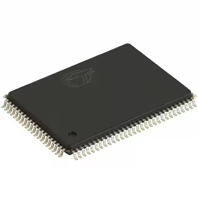
100 MHz synchronous SRAM with NoBL pipeline
The Cypress CY7C1371KV33-100AXC is an 18 Mbit synchronous SRAM from the NoBL™ family, organized as 512K words by 36 bits. It clocks at 100 MHz and delivers an 8.5 ns access time from the first address, with subsequent pipelined reads at the full clock rate. The 36-bit data bus maps cleanly to 32-bit processors needing parity or to 36-bit DSP datapaths without splitting the word across two chips. The parallel memory interface uses standard synchronous control signals (clock, chip enable, write enable, output enable, byte write selects) common to most mid-density SRAM controllers. It is not specified for industrial or automotive environments.
The 100 MHz clock sets the peak throughput for back-to-back pipelined transactions: one 36-bit word per cycle after the initial latency. For random access patterns (e.g., cache-line refill after a miss), the access time dominates; for sequential bursts, the clock rate dominates. NoBL (No Bus Latency) means the part can start a new read or write on every clock cycle without dead cycles for bus turnaround. This eliminates the idle cycle that conventional synchronous SRAMs insert when switching from read to write, improving sustained throughput in mixed-transaction workloads.
The 100-pin LQFP (also supplied as 100-TQFP, 14x20 mm body) uses a 0.5 mm fine-pitch leadframe. It is a peripheral-lead package, so rework with hot air is straightforward — no underfill or preheat ramp required beyond standard JEDEC MSL precautions. The lead pitch demands a clean solder-paste stencil and careful alignment during reflow, but the package itself is forgiving for hand rework with a fine-tip iron or hot-air pencil. Surface-mount only; no through-hole variant. The 14x20 mm footprint fits standard PCB layouts for 100-pin QFP SRAMs.