Dual-port arbitration and bus timing
The CY7C136E-25JXIT: In a dual-port SRAM, both ports can read or write any memory location simultaneously — the 25 ns spec is the time from address valid to data valid on the bus, and it defines the minimum cycle time for back-to-back accesses. For a system clocked at 40 MHz (25 ns period), the access time consumes the entire cycle, so wait states are needed if the bus master runs faster than the memory's native speed.
Industrial temperature and 5 V logic domain
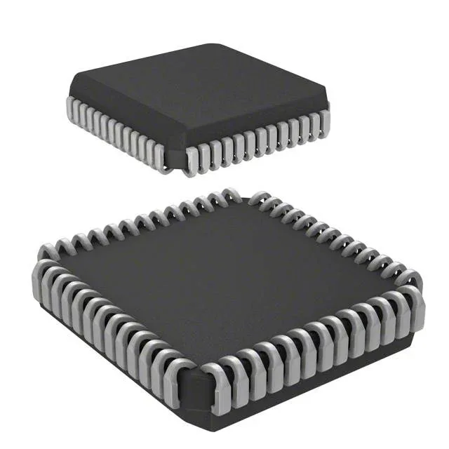
The 52-PLCC (J-Lead) package is a through-hole-reflow-friendly footprint; the leads are visible for inspection and rework, unlike a BGA that requires X-ray. The supplier device package is 52-PLCC (19.13x19.13 mm).
Infineon lists the CY7C136E-25JXIT as Obsolete. For a BOM that requires this exact dual-port SRAM in the 52-PLCC footprint, the procurement path is a last-time-buy or surplus sourcing — there is no pin-compatible drop-in replacement from Infineon's current active portfolio.