3.5 ns access time — timing closure for the bus
At a 166 MHz clock (6 ns period), this leaves roughly 2.5 ns of setup/hold margin for the controller — tight but workable with a well-terminated PCB layout. If your system runs at a lower clock rate, the margin improves proportionally. This is the spec that determines whether the SRAM can keep up with your ASIC or FPGA without wait states.
256K x 32 organization — why the width matters
The 8Mbit memory is organized as 256K words of 32 bits each. A x32 interface is common in networking and telecom gear where a wide data bus matches the processor or packet buffer width directly — no byte-lane muxing needed. For a 32-bit CPU or a 32-bit DDR controller, this part connects without glue logic. The parallel interface uses a synchronous burst mode, so the controller must supply a clock and handle the pipeline latency.
Commercial temperature — indoor only
Not rated for automotive under-hood, outdoor base stations, or industrial enclosures without active cooling. If your application sees -40°C or +85°C, this part is not the fit — you need an industrial-temperature synchronous SRAM in the same family.
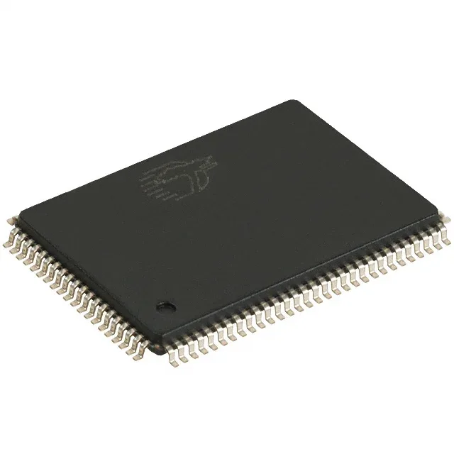
Supplied in a 100-lead TQFP (14x20 mm body) — a standard fine-pitch QFP with 0.5 mm lead pitch. Surface-mount only. The 100-TQFP footprint is shared across the CY7C1368 family, so a board designed for the C-version will accept a compatible D-version without layout changes.