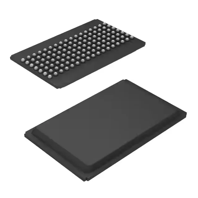
119-ball BGA footprint and board integration
The CY7C1366C-166BGC ships in a 119-ball PBGA (plastic ball grid array) with a 14x22 mm body. The 1.27 mm ball pitch is routable on a four-layer board without microvias, but the 119-ball count demands at least two inner signal layers for fan-out. Tray packaging is the standard delivery format for BGA devices this size — the trays index directly into pick-and-place feeders without tape-and-reel conversion. Moisture sensitivity level should be verified from the lot date code before reflow; a 24-hour bake at 125°C is typical if the floor life has been exceeded.
166 MHz synchronous SRAM — timing and organization
At 166 MHz clock frequency with a 3.5 ns access time, this synchronous SDR SRAM delivers one word per clock cycle in pipelined read mode — the 256K x 36 organization yields 9 Mbit total density. The 36-bit word width maps directly to a 32-bit data bus plus four parity or ECC bits, common in network switch buffers and cache applications where the extra width avoids a second device. The parallel memory interface uses registered address and control inputs — setup and hold times relative to the rising clock edge must be met at the BGA balls, not at the FPGA or ASIC die. The 3.5 ns access time is the clock-to-data-valid delay; at 166 MHz (6 ns period), this leaves 2.5 ns for the receiving device's input setup, which constrains the PCB trace length to under 50 mm on standard FR4 without termination.
Infineon Technologies lists the CY7C1366C-166BGC as Obsolete. The part is sourced through independent distribution channels — quantities are lot-specific and confirmed at RFQ. Buyers should verify date codes and package condition (BGA solder ball oxidation) before committing to a reel or tray quantity. For new designs, a pin-compatible synchronous SRAM in the same 119-PBGA footprint with a 166 MHz or higher clock rating should be evaluated as a replacement.