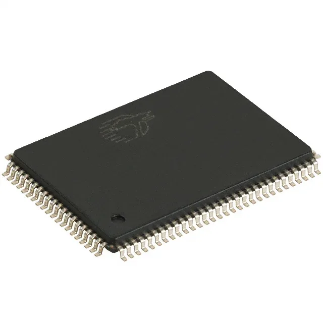
256K x 36 synchronous SRAM — 166 MHz pipeline
The CY7C1366C-166AXC is a 9Mbit synchronous SDR (single-data-rate) SRAM organised as 256K words by 36 bits. The 166 MHz clock rate yields a 3.5 ns access time from clock rise, which sets the read-to-data-valid window for the downstream logic — the pipeline depth means the first read incurs the full latency, but subsequent back-to-back reads issue one per clock cycle. The 36-bit-wide data bus maps naturally to 32-bit processor buses with four parity/ECC bits, or to a 36-bit DSP word. The parallel interface eliminates serialisation overhead, so the throughput ceiling is the clock rate times the bus width: 166 MHz × 36 bits = 5.976 Gbit/s raw bandwidth.
Supply rails and temperature grade
For extended-temperature designs this part is not rated; the industrial-grade sibling in the same family would be the correct call.
Package and footprint
Supplied in a 100-lead LQFP (EIAJ standard), the supplier device package is the 100-TQFP with a 14×20 mm body. The 0.5 mm pitch requires a four-layer PCB for reliable fan-out of the inner rows — two-layer boards will struggle to route the 36 data lines plus address and control without via congestion. Tray packaging is the standard delivery format for this order code.
Last Buy — planning the BOM transition
Infineon has placed the CY7C1366C-166AXC into Last Buy status. This means the manufacturer will accept final orders for a defined window, after which the part is discontinued with no further production. Any new design should avoid this order code; existing production that depends on it should secure last-time-buy quantities or qualify a replacement before the cutoff. The closest functional replacement would be a pin-compatible synchronous SRAM from the same Cypress/Infineon family with the same 100-TQFP footprint — confirm the exact ordering code against the BOM position before committing.