What the 133 MHz clock and 6.5 ns access time mean for your bus
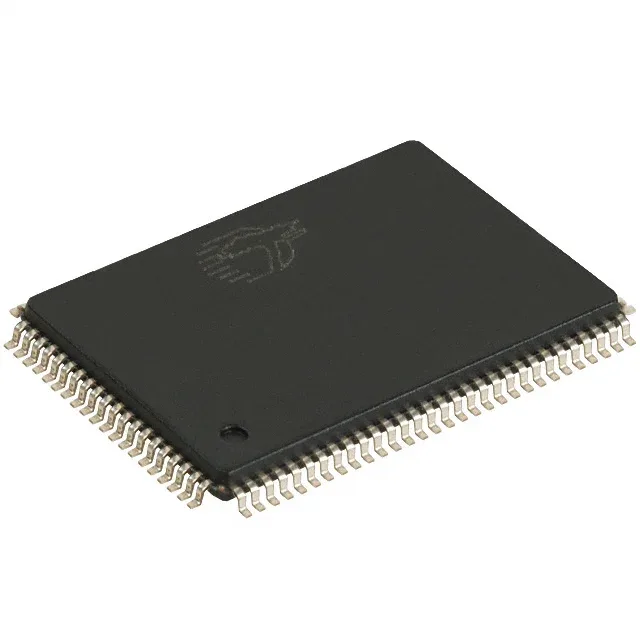
The CY7C1363C-133AJXC is a 9 Mbit synchronous SRAM organized as 512K x 18 bits. The 133 MHz clock frequency means the memory can deliver one 18-bit word per clock cycle in burst mode, which is the standard interface for high-speed cache or buffer applications in networking and telecom equipment. The 6.5 ns access time is the time from the address being latched to data appearing on the outputs; at 133 MHz the clock period is about 7.5 ns, so the access time leaves roughly 1 ns of setup margin for the downstream logic — tight, but within spec for a properly terminated bus.
Supply voltage and interface
The parallel memory interface is a 18-bit data bus plus address and control signals; the 512K x 18 organization means 19 address lines. The base product number is CY7C1363, which helps when searching for related variants or errata documents.
Infineon lists this part as Obsolete. Availability is lot-specific and confirmed at RFQ; pricing is market-driven and quoted per request.