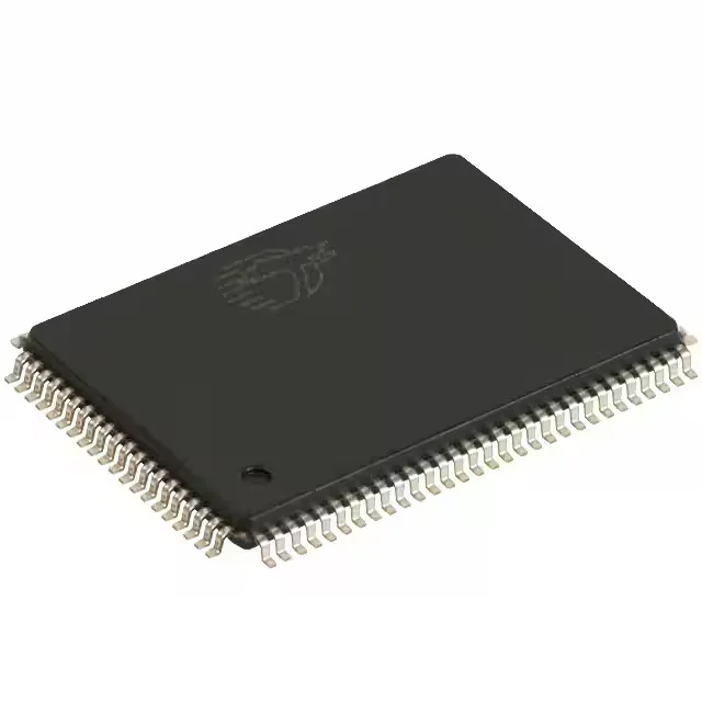
9 Mbit synchronous SRAM with a 36-bit datapath
The Cypress CY7C1361C-133AJXC is a 9 Mbit synchronous pipelined SRAM organized as 256K words by 36 bits. It clocks at 133 MHz with a 6.5 ns access time from clock rising edge, which means the read data is valid on the bus within one clock cycle at that frequency. The part runs from a 3.135V to 3.6V supply, so it sits comfortably on a nominal 3.3V rail with margin for regulator droop. The parallel interface uses standard synchronous SRAM control signals — address, data, chip enable, output enable, and byte write enables for the four byte lanes.
For existing BOM lines that need this exact part, supply runs through independent distribution — surplus, new-old-stock, and broker inventory. The 'C' revision brought a faster clock speed and tighter access time; the 'B' runs at lower frequency. Verify the timing parameters against your bus budget before substituting — the 'B' may not meet a 133 MHz requirement.
133 MHz clock and 6.5 ns access — reading the timing budget
The 133 MHz clock rate corresponds to a 7.5 ns cycle period. The 6.5 ns access time (clock to data valid) leaves 1.0 ns of setup margin at the receiver in a zero-delay ideal case. In practice, board trace delay, clock skew, and output loading eat into that margin. This part is designed for systems with tight timing closure — you will need controlled-impedance traces and matched clock distribution to hold the bus at 133 MHz. The pipelined architecture adds one cycle of latency on reads, which the memory controller must account for in its wait-state logic.
100-pin TQFP — footprint and reflow notes
The package is a 100-lead TQFP with 0.5 mm pitch, body size 14 mm x 20 mm. The part is surface-mount only. No MSL rating is in the record, but Cypress typically rated these synchronous SRAMs at MSL 3; verify the moisture-sensitive label on the actual reel or tray before reflow. If the pouch seal is compromised, bake at 125°C for 48 hours to avoid popcorning.