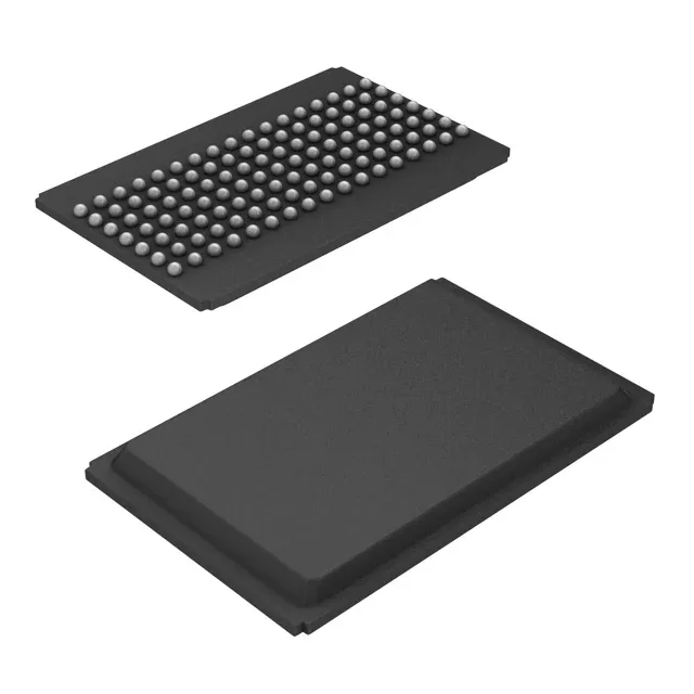
Infineon Technologies CY7C1356C-166BGC — Memory (DRAM / SRAM / Flash / EEPROM)

Infineon CY7C1356C-166BGC 9Mbit NoBL SRAM, 166 MHz

MPNCY7C1356C-166BGC
Obsolete

Infineon Technologies NoBL™ synchronous SRAM, CY7C1356C-166BGC, 9Mbit (512K x 18), 166 MHz clock, 3.5 ns access, 119-PBGA (14x22 mm), tray.

Independent supplier — new & surplus stockAuthenticity-screened · ESD-safe packingListing updated Jul 2026

Specifications

CY7C1356C-166BGC specifications
ParameterValue
SeriesNoBL™
Memory typeVolatile
MountingSurface Mount
Supply voltage3.135V ~ 3.6V
Clock frequency166 MHz
Memory interfaceParallel
Operating temperature0°C ~ 70°C (TA)
PackageTray
TechnologySRAM - Synchronous, SDR
Access time3.5 ns
Memory size9Mbit
Memory formatSRAM
Case119-BGA
Memory organization512K x 18

Product details

166 MHz synchronous SRAM — the speed-density tradeoff

The CY7C1356C-166BGC is a 9 Mbit synchronous SRAM from Infineon's NoBL (No Bus Latency) family, organized as 512K x 18 bits. It clocks at 166 MHz with a 3.5 ns access time — the flow-through pipeline means the first read address appears on the data bus one cycle after the read command, then a new word every clock edge thereafter. For a cache line fill or a FIFO buffer running at that rate, the 3.5 ns access buys enough timing margin to avoid wait states in a typical 100-133 MHz bus.

Infineon has marked this part Obsolete.

Housed in a 119-ball PBGA (14x22 mm body), the 1.0 mm ball pitch is hand-solderable with a hot-air rework station and a stencil — not a breadboard-friendly part, but a rework lab can replace it with practice.

Frequently asked questions

What is the closest pin-compatible alternative to CY7C1356C-166BGC?

No official pin-compatible successor or cross-reference is recorded from Infineon. A functional replacement would require a board spin — the package and pinout differ across the synchronous SRAM families. Confirm the BOM position before committing.