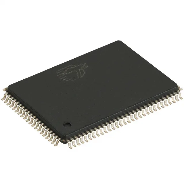
Infineon Technologies CY7C1350G-200AXI — Memory (DRAM / SRAM / Flash / EEPROM)

Infineon CY7C1350G-200AXI 4.5Mbit SRAM, 200 MHz, 2.8 ns

MPNCY7C1350G-200AXI
Obsolete

Infineon Technologies NoBL™ synchronous SRAM, CY7C1350G-200AXI, 4.5 Mbit (128K x 36), 200 MHz clock, 2.8 ns access, 3.3 V, 100-LQFP, industrial temp.

$6.9104Ref. price · indicative, final on quote
Independent supplier — new & surplus stockAuthenticity-screened · ESD-safe packingListing updated Jul 2026

Specifications

CY7C1350G-200AXI specifications
ParameterValue
SeriesNoBL™
Memory typeVolatile
MountingSurface Mount
Supply voltage3.135V ~ 3.6V
Clock frequency200 MHz
Memory interfaceParallel
Operating temperature-40°C ~ 85°C (TA)
PackageTray
TechnologySRAM - Synchronous, SDR
Access time2.8 ns
Memory size4.5Mbit
Memory formatSRAM
Case100-LQFP
Memory organization128K x 36

Product details

200 MHz synchronous SRAM in 100-LQFP

The CY7C1350G-200AXI is a 4.5 Mbit synchronous SRAM from Infineon's NoBL™ (No Bus Latency) family, organized 128K x 36 and clocked at 200 MHz. The 2.8 ns access time means the first read word appears on the data bus within three clock edges of the address — the pipeline depth is three cycles, so the latency is deterministic at 15 ns at 200 MHz. This part sits in the synchronous SRAM slot of a high-throughput memory map, typically a deep FIFO or cache buffer in networking or industrial control.

Infineon lists the CY7C1350G-200AXI as Obsolete.

The 100-TQFP package (14x20 mm body) has a 0.5 mm pitch that routes cleanly on a four-layer board with the VDDQ and VSS decoupling placed within 5 mm of each supply pin pair.

Frequently asked questions

What is the memory organization and clock speed of the CY7C1350G-200AXI?

The CY7C1350G-200AXI is organized as 128K x 36 (4.5 Mbit total) and runs at a 200 MHz clock frequency with a 2.8 ns access time.