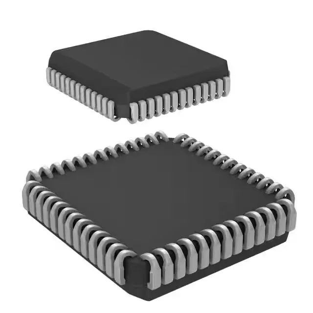
Infineon Technologies CY7C131-55JXI — Memory (DRAM / SRAM / Flash / EEPROM)

Infineon CY7C131-55JXI Dual-Port SRAM, 8Kbit, 55 ns, 52-PLCC

MPNCY7C131-55JXI
Obsolete

Infineon CY7C131-55JXI, Dual-Port Asynchronous SRAM, 8Kbit (1K x 8), 55 ns access time, Parallel interface, 4.5 V to 5.5 V supply, -40°C to 85°C, 52-PLCC, Tube.

Independent supplier — new & surplus stockAuthenticity-screened · ESD-safe packingListing updated Jul 2026

Specifications

CY7C131-55JXI specifications
ParameterValue
Memory typeVolatile
MountingSurface Mount
Supply voltage4.5V ~ 5.5V
Memory interfaceParallel
Operating temperature-40°C~85°C(TA)
PackageTube
TechnologySRAM - Dual Port, Asynchronous
Access time55 ns
Memory size8Kbit
Memory formatSRAM
Case52-LCC (J-Lead)
Memory organization1K x 8
Write cycle time - word, page55ns

Product details

55 ns dual-port SRAM for asynchronous cross-domain buffering

The Infineon CY7C131-55JXI is a 55 ns asynchronous dual-port SRAM organized as 1K x 8 bits, giving 8 Kbit of volatile storage accessible from two independent ports.

The 52-lead PLCC package with J-leads (52-PLCC, 19.13 mm square body) is a surface-mount form factor that typically requires a PLCC socket for prototyping or a reflow profile tuned for J-lead solder joints. The J-lead footprint offers good visual inspectability after soldering, unlike a BGA.

Infineon lists the CY7C131-55JXI as obsolete. New designs should migrate to a current-production dual-port SRAM or to a different dual-port memory architecture.

Frequently asked questions

What is the access time of CY7C131-55JXI?

The access time is 55 ns, which defines the maximum bus clock rate (roughly 18 MHz without wait states) and the read/write cycle timing margin for your design.

Where can I buy CY7C131-55JXI?

Submit an RFQ to confirm current availability and pricing — each lot is quoted to order.