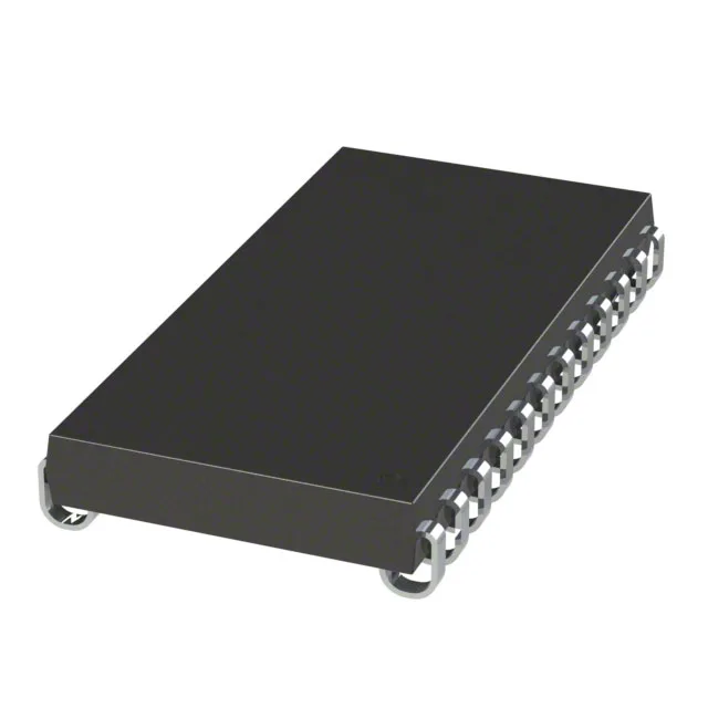
The CY7C128A-25VC is a Cypress 16Kbit asynchronous SRAM organized as 2K x 8, with a 25 ns access time that sets the read-cycle floor for the memory bus. In a legacy 5V system, that 25 ns window means the CPU or controller can sample data 25 ns after asserting the address — no wait states needed if the processor's memory cycle is 40 ns or slower. The parallel interface is straightforward: address, chip enable, output enable, and bidirectional data lines, no clock or refresh overhead. This part is volatile, so contents are lost at power-down.
5V-only supply — not a drop-in for 3.3V designs
Supply range is 4.5V to 5.5V, a pure 5V part. If your board runs a 3.3V memory bus, this SRAM will not work without level shifters on every address, data, and control line — and the 5V input thresholds on the chip enable and output enable pins mean the 3.3V logic-high may not reliably reach VIH.