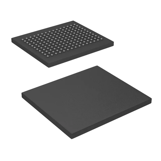
It uses a parallel memory interface and is housed in a 165-LBGA surface-mount package. This class of high-speed SRAM is designed for networking equipment, telecom line cards, test-and-measurement instruments, and high-end compute systems where low-latency, high-bandwidth data buffering is critical — think packet buffers, look-up tables, and cache memory in FPGA or ASIC companion roles. The 400 MHz clock rate delivers a peak bandwidth of 3.2 GB/s on a 36-bit bus, which is what makes it suitable for those throughput-hungry applications.
The 400 MHz clock is the headline number. For a QDR II architecture, that means two data transfers per clock cycle on both read and write ports, effectively quadrupling the data rate relative to a single-data-rate SRAM at the same clock. In practice, this part sustains back-to-back read-write transactions with no dead cycles, which is exactly what a high-speed data converter or a network processor needs to avoid stalling the pipeline. This is not a part you breadboard; it belongs on a multi-layer board with a solid power plane.
If you are designing a new system, avoid this part; if you are supporting an existing build, secure inventory through a trusted independent distributor that can verify date codes and authenticity before shipment.
Package and temperature — board-level reality
If your system sees ambient above 70°C or below freezing, this part is not the right fit.