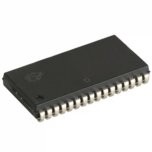
128K x 8 — the byte-wide bus constraint
The 128K x 8 organization means this SRAM presents an 8-bit data word at each address. If your processor or FPGA memory controller expects a 16-bit or 32-bit wide memory, you'll need two or four of these devices in parallel, plus the matching chip-select and address decoding. For an 8-bit microcontroller or a narrow DMA channel, it's a direct fit with no glue logic.
The 'I' suffix in the order code signals the industrial temperature grade — a common procurement checkpoint when a BOM is being qualified for an extended-temperature environment.
32-SOJ package — footprint and rework notes
Housed in a 32-BSOJ package (0.400" body width, 10.16 mm), this is a J-lead surface-mount part. The J-lead footprint is less prone to tombstoning than gull-wing, but the leads are hidden under the body, making visual inspection of solder joints difficult. If your rework station is set up for TSOP or QFP, check that your hot-air nozzle can reach the J-lead fillet. The supplier device package is 32-SOJ.
Write cycle time matches read access
In a system that does back-to-back read-modify-write operations — like a cache-line fill-and-invalidate — the symmetric timing simplifies the controller state machine.
The base product number is CY7C109, and the 'D' revision is the current die stepping.