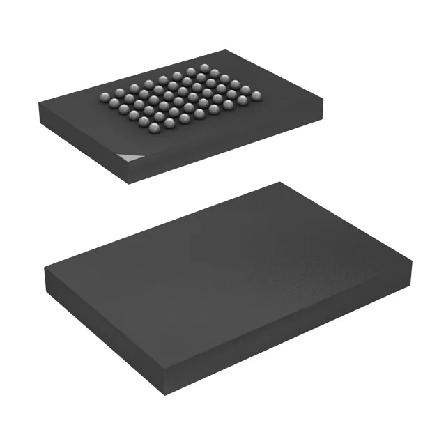
32Mbit asynchronous SRAM for industrial and telecom systems
The 12 ns access time means the host processor can complete a read or write cycle in a single bus transaction at clock rates up to roughly 83 MHz, assuming zero wait states — a common fit for 66 MHz and 80 MHz buses on older PowerPC, ARM9, or x86 embedded controllers that still use a byte-wide parallel SRAM interface.
12 ns access time — timing margin on the bus
The 12 ns access time and 12 ns write cycle time are the same figure, which simplifies the timing budget: the part can sustain back-to-back reads or writes at a 12 ns cycle period. For a system architect sizing the memory bus, that 12 ns window includes address setup, chip-select propagation, and data-out valid. On a 66 MHz bus (15 ns period), the 12 ns access leaves 3 ns of margin for PCB trace delay and buffer skew — tight but workable with careful layout. The write cycle time being identical to the read access means the controller does not need separate wait-state configurations for read versus write transactions.
48-ball FBGA — footprint and rework considerations
The part comes in a 48-ball FBGA (8x9.5 mm) with a 0.8 mm ball pitch typical of this density class.
For a procurement buyer qualifying this into a production BOM, there is no last-time-buy deadline to track. The part is the tape-and-reel ordering code (the 'T' suffix), which is the preferred format for automated pick-and-place assembly lines. The tray variant (-12BAXI) is the same silicon in a different shipping medium, so the BOM can specify either depending on the assembly house's feeder preference.