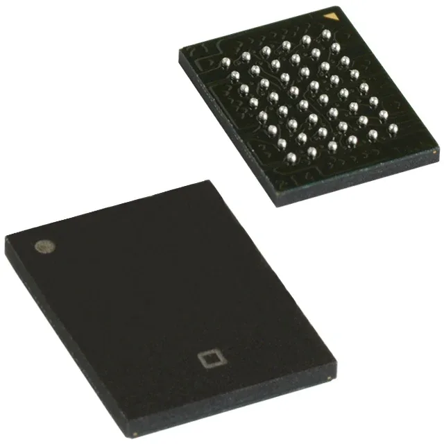
16Mbit asynchronous SRAM for embedded buffering
The CY7C1069GN30-10BVXIT is a 16Mbit asynchronous SRAM from Infineon, organized as 2M x 8, with a 10 ns access time. That 10 ns window sets the bus cycle margin — at a 100 MHz bus clock, the memory responds within one clock edge, leaving headroom for PCB trace delay and signal settling. The supply range spans 2.2V to 3.6V, so this part sits on either a 2.5V or 3.3V rail without an external regulator.
The 10 ns access time and 10 ns write cycle time mean the SRAM can complete a read or write in a single 100 MHz bus cycle. For a system architect, this eliminates the need for wait states on a 100 MHz memory bus, keeping the CPU fed without stalling. The parallel memory interface is straightforward — no address-multiplexing overhead, just chip enable, output enable, and write enable strobes. This simplifies the FPGA or MCU glue logic compared to a synchronous burst SRAM.
Infineon lists this part as Active. The 48-VFBGA (6x8 mm) package is a fine-pitch BGA — the ball pitch is 0.75 mm or 0.80 mm depending on the specific footprint variant. For the rework lab tech: this demands a pre-bake at 125°C for 8 hours if the moisture-barrier bag is breached, and a hot-air profile with a top-side thermocouple on the package body.
Board-fit and footprint notes
Surface-mount 48-VFBGA, 6x8 mm body. The 0.50 mm or 0.75 mm ball pitch (verify the specific footprint drawing) requires a 4-layer PCB with microvias for fan-out. The thermal pad on the bottom of the package is not electrically connected — it is a mechanical reference, not a heatsink. Decoupling: place a 100 nF ceramic capacitor within 2 mm of each VDD ball pair, plus a 10 µF bulk cap per supply rail. The 2.2V–3.6V range means the I/O levels track the supply — no separate VDDQ rail.