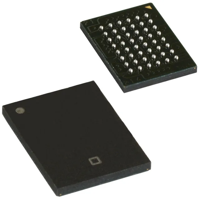
16 Mbit async SRAM with 10 ns access — what that means for bus timing
The CY7C1069GN30-10BVXI: That 10 ns window sets the minimum read cycle time — the controller must sample data within that window after asserting the address, or the bus margin collapses. This part fits best in asynchronous interfaces where the controller can tolerate a full 10 ns address-to-data delay. The write cycle time matches the read at 10 ns, meaning back-to-back writes run at the same speed as reads — no dead cycle penalty on mixed-access sequences.
48-VFBGA footprint — what the board needs
The 48-VFBGA (6x8 mm) package uses a 0.5 mm ball pitch — standard for this density. Surface-mount only — no socket option.
The base product number CY7C1069 covers multiple speed and package variants; this -10BVXI suffix (10 ns, VFBGA, industrial temp) is the standard production grade.
Parallel interface — bus compatibility check
The memory interface is parallel with a standard asynchronous SRAM control set: chip enable, output enable, write enable. No clock, no address latch — the controller drives the address bus and waits the 10 ns access time before strobing data. This simplicity makes it a drop-in replacement for any 2M x 8 asynchronous SRAM socket with the same pinout, but the 48-VFBGA package is unique to the Cypress/Infineon family — confirm the ball map against the PCB footprint before committing.