Package and footprint — 48-VFBGA (6x8 mm)
The 48-VFBGA (6x8 mm) package is a fine-pitch BGA that saves board area compared to a 44-pin TSOP, but it requires a controlled impedance layout and at least four-layer PCB for the signal escape.
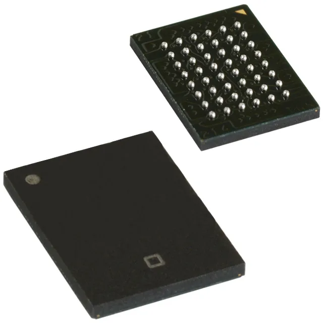
Cypress Semiconductor CY7C1069G30-10BVXI, 16Mbit asynchronous SRAM, 10 ns access time, 2.2V–3.6V supply, parallel interface, -40°C to 85°C, 48-VFBGA (6x8 mm) tray.
| Parameter | Value |
|---|---|
| Memory type | Volatile |
| Mounting | Surface Mount |
| Supply voltage | 2.2V ~ 3.6V |
| Memory interface | Parallel |
| Operating temperature | -40°C ~ 85°C (TA) |
| Package | Tray |
| Technology | SRAM - Asynchronous |
| Access time | 10 ns |
| Memory size | 16Mbit |
| Memory format | SRAM |
| Case | 48-VFBGA |
| Memory organization | 2M x 8 |
| Write cycle time - word, page | 10ns |
The 48-VFBGA (6x8 mm) package is a fine-pitch BGA that saves board area compared to a 44-pin TSOP, but it requires a controlled impedance layout and at least four-layer PCB for the signal escape.
The access time is 10 ns, which is the cycle time for both read and write operations (word and page write cycle time is also 10 ns).
The closest functional alternative is the CY7C1061G30-10BVXI, which is also a 16Mbit asynchronous SRAM with 10 ns access time and the same 48-VFBGA package, but organized as 1M x 16 instead of 2M x 8. The wider data bus changes the pinout and board layout, so verify the memory controller's bus width before substituting.