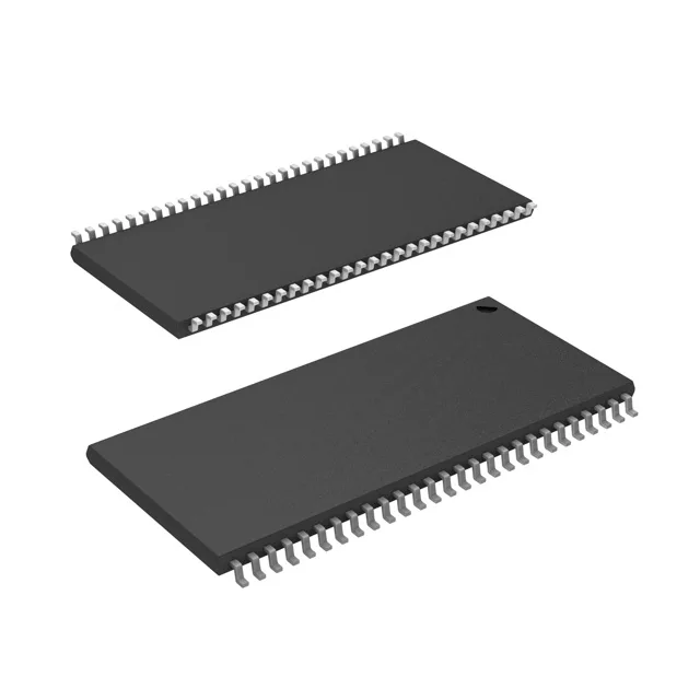
What this async SRAM does on the bus
The part comes in a 54-TSOP II package. This is a workhorse fast SRAM for applications that need deterministic, no-wait-state reads and writes — think networking equipment buffers, industrial controller cache, or FPGA block-RAM expansion where the bus can tolerate a byte-wide memory.
10 ns access time — timing closure for the bus
In a system with a 50 MHz to 66 MHz bus clock, that 10 ns window sets the address-to-data valid delay. For a designer, this means the part can keep up with a fast 8-bit microcontroller or a medium-speed FPGA memory controller without inserting wait states. If your bus runs faster than 66 MHz, you will need to account for the access time in the timing budget — the 10 ns figure is the max from address change to data valid, not a cycle time.
16 Mbit density and 2M x 8 organization
The 16 Mbit density and 2M x 8 organization mean the part provides 2 megawords of 8-bit data. This is a natural fit for 8-bit microcontroller data memory, a small frame buffer, or a look-up table in a DSP system. The byte-wide interface simplifies PCB routing compared to a x16 or x32 part, and the 54-TSOP II footprint is a standard surface-mount package that many memory controllers support. If you need more than 2 MB of SRAM, you will either stack multiple parts or move to a higher-density synchronous SRAM — but for a 2 MB working memory, this is a compact, single-chip solution.
Industrial temperature and 5V supply
If your design has moved to 3.3V logic, this part will need a 5V supply rail or a level translator on the address/data bus.
The base product number is CY7C1069, and the G suffix indicates the latest die revision.