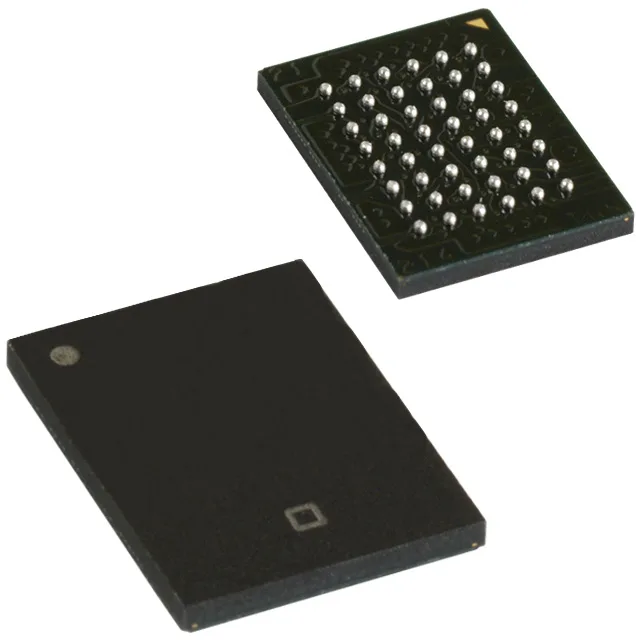
Infineon Technologies CY7C1069G-10BVXI — Memory (DRAM / SRAM / Flash / EEPROM)

Infineon CY7C1069G-10BVXI 16Mbit Async SRAM, 10 ns, 48-VFBGA

MPNCY7C1069G-10BVXI
Active

Infineon CY7C1069G-10BVXI, asynchronous SRAM, 16 Mbit (2M x 8), 10 ns access time, parallel interface, 4.5 V to 5.5 V supply, -40°C to 85°C, 48-VFBGA (6x8 mm), Tray.

$27.5000Ref. price · indicative, final on quote
StockContact for availability
MOQ1 pcs
  • 100% new & originalTraceable channels only — no refurbs, no pulls, no remarked parts.
  • Date & lot codes on quoteStated per line before you commit; label photos on request.
  • MSL-compliant ESD packingMoisture-sealed bags with indicator cards; reels photo-verified.
  • PayPal buyer protectionPay by T/T, PayPal or Payoneer — card payments covered end to end.

Specifications

CY7C1069G-10BVXI Technical Specifications
ParameterValue
Memory typeVolatile
Mounting typeSurface Mount
Voltage4.5V ~ 5.5V
Memory interfaceParallel
Operating temperature-40°C ~ 85°C (TA)
PackageTray
TechnologySRAM - Asynchronous
Access time10 ns
Memory size16Mbit
Memory formatSRAM
Case48-VFBGA
Memory organization2M x 8
Write cycle time - word, page10ns

Product details

16 Mbit async SRAM, 10 ns — fits the fast scratchpad slot

The Infineon CY7C1069G-10BVXI is a 16 Mbit asynchronous SRAM organized 2M x 8, with a 10 ns access time and a parallel interface. It operates from a 4.5 V to 5.5 V supply over the industrial temperature range of -40°C to 85°C. Housed in a 48-VFBGA (6x8 mm) package, this part is aimed at applications requiring fast, predictable read/write cycles without refresh overhead — think cache tags, packet buffers, DSP scratchpad memory, or FPGA block-RAM expansion in telecom line cards and industrial controllers.

10 ns access time — what it means for the bus

Access time is 10 ns. Write cycle time is also 10 ns.

Industrial temperature and 5 V supply — deployment context

Operating temperature range is -40°C to 85°C. Supply voltage range is 4.5 V to 5.5 V.

Lifecycle and sourcing

The manufacturer lists the CY7C1069G-10BVXI as Active. No EOL notice or last-time-buy schedule is in effect. This part is sourced and quoted to order against an RFQ through independent distribution; availability and current pricing are confirmed at quote time.

Frequently asked questions

Is CY7C1069G-10BVXI obsolete or nearing end of life?

No — the manufacturer lists this part as Active with no EOL notice in effect. It remains a valid BOM line for new production and repair stock.

What is the datasheet for CY7C1069G-10BVXI?

The datasheet covers the full electrical specifications, timing diagrams, and package drawing for this 16 Mbit asynchronous SRAM. It is available from the manufacturer's website or through distribution upon request.

What is the pinout of CY7C1069G-10BVXI?

The pinout is defined in the datasheet for the 48-VFBGA package. The device uses a standard asynchronous SRAM pin arrangement with address, data, chip enable, output enable, and write enable signals.