16 Mbit async SRAM with 10 ns access — the bus-timing decision
This wide-word organization maps directly to a 32-bit processor bus without external byte-lane muxing, saving two to four octal latches and their associated propagation delay. The 10 ns access sets the ceiling for the memory-read cycle — a 100 MHz bus with a 10 ns cycle time leaves zero margin for address-to-data setup; at 66 MHz (15 ns cycle) the part fits with a 5 ns timing budget for address decode and board trace skew.
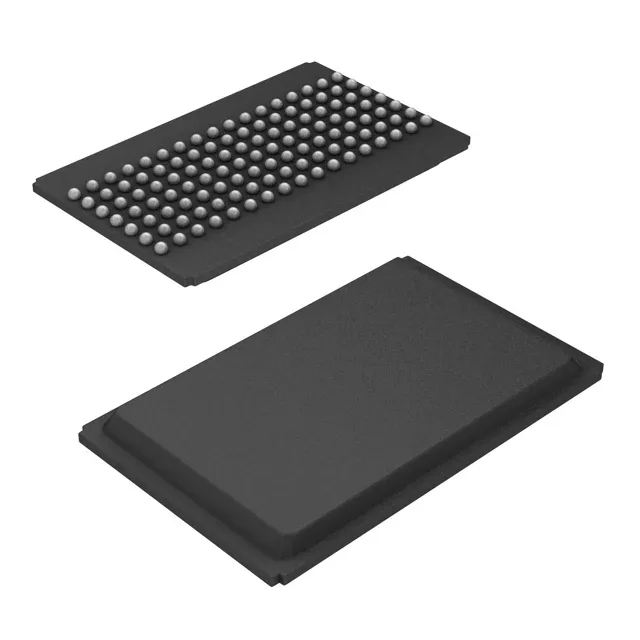
119-PBGA footprint — layout and rework notes
Housed in a 119-ball PBGA measuring 14x22 mm, the part demands a multi-layer PCB with at least four signal layers to fan out the 32 data lines plus address and control. Decouple with a 100 nF ceramic per supply pin pair, placed within 2 mm of the ball array. The BGA is MSL 3 — if the moisture-barrier bag has been open longer than the floor-life window, bake at 125°C for 48 hours before reflow. For rework, a bottom-side preheat at 150°C and a focused hot-air nozzle at 240°C peak (lead-free profile) typically lifts the part cleanly; inspect for solder-ball bridging under X-ray.
For dual-sourcing resilience, the base product number CY7C1062 covers multiple speed and temperature variants sharing the same 119-BGA footprint — a -10 (10 ns) and -12 (12 ns) option exist, though the -10 is the fastest in the family.