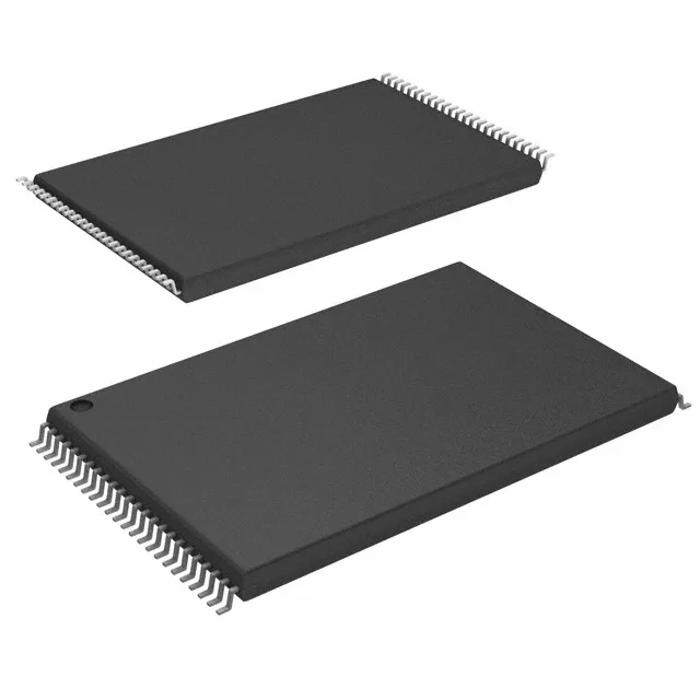
Infineon Technologies CY7C1061GN30-10ZXI — Memory (DRAM / SRAM / Flash / EEPROM)

Infineon CY7C1061GN30-10ZXI SRAM, 16Mbit, 10 ns, 48-TFSOP

MPNCY7C1061GN30-10ZXI
Active

Infineon CY7C1061GN30-10ZXI, asynchronous SRAM, 16Mbit (1M x 16), 10 ns access time, 2.2V–3.6V supply, parallel interface, -40°C to 85°C, 48-TFSOP (TSOP I) tray.

$29.5141Ref. price · indicative, final on quote
Independent supplier — new & surplus stockAuthenticity-screened · ESD-safe packingListing updated Aug 2026

Specifications

CY7C1061GN30-10ZXI specifications
ParameterValue
Memory typeVolatile
MountingSurface Mount
Supply voltage2.2V ~ 3.6V
Memory interfaceParallel
Operating temperature-40°C ~ 85°C (TA)
PackageTray
TechnologySRAM - Asynchronous
Access time10 ns
Memory size16Mbit
Memory formatSRAM
Case48-TFSOP (0.724\", 18.40mm Width)
Memory organization1M x 16
Write cycle time - word, page10ns

Product details

Industrial temperature range — where it works

The 2.2V to 3.6V supply range covers both 2.5V and 3.3V rails, so it drops into existing 3.3V designs or low-power 2.5V systems without a regulator change.

Housed in a 48-TFSOP (0.724", 18.40 mm width) — the standard TSOP I footprint for 48-pin SRAMs. The supplier device package is 48-TSOP I, which is the same mechanical outline.

Lifecycle status

Infineon lists the CY7C1061GN30-10ZXI as Active. The base product number CY7C1061 covers a family of 16 Mbit asynchronous SRAMs with different speed grades and temperature ranges; the -10ZXI suffix selects the 10 ns industrial-grade variant in TSOP I.

Frequently asked questions

What is the access time of CY7C1061GN30-10ZXI?

The access time is 10 ns for both read and write operations. That means data appears on the bus within 10 ns of the address going valid, and a full write cycle also completes in 10 ns.

Is CY7C1061GN30-10ZXI RoHS compliant?

The part is lead-free and RoHS-compliant per Infineon's standard product marking. No separate RoHS certificate is needed for this order code.