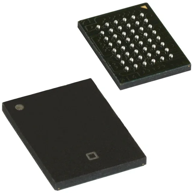
10 ns asynchronous SRAM for industrial memory subsystems
It operates from a 2.2V to 3.6V supply, making it compatible with both 2.5V and 3.3V logic families without external level shifters. The parallel interface is straightforward to route on a PCB, and the 48-VFBGA (6x8 mm) footprint keeps the board area compact.
10 ns access — what it buys the timing budget
In practice, this gives the designer headroom when routing the address and data buses across a board: trace delays, capacitive loading from multiple memory banks, and setup/hold requirements of the host controller all eat into the timing budget. With a 10 ns part, you can often avoid adding pipeline registers or slowing the system clock.
That covers cold-start at -40°C in an outdoor cabinet and the self-heating inside a sealed enclosure on a factory floor. The 2.2V to 3.6V supply range means the part can run from a 2.5V rail (common in low-power FPGA designs) or a 3.3V rail (standard for legacy processor buses) without a separate regulator. The 1M x 16 organization is well suited for 16-bit data buses, giving a single-chip memory solution for many MCU and DSP applications.
Surface-mount assembly is standard, but the small ball size means the PCB pad design and solder-paste volume need to be controlled to avoid head-in-pillow defects.
For a production BOM this removes the risk of a sudden last-time-buy.