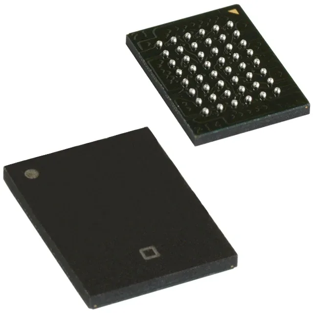
Memory density and timing for the data path
The CY7C1061GE30-10BVXI is a 16 Mbit asynchronous SRAM organized as 1M x 16 bits, accessed through a parallel interface. The 10 ns access time and matching 10 ns write cycle time (word, page) mean the part can keep up with a processor bus running at 100 MHz without wait states — the data sheet's nominal timing is the ceiling for back-to-back reads. The wide range also gives headroom for a lightly regulated rail — the minimum 2.2 V is the dropout floor, not a recommendation to design at the edge.
Housed in a 48-ball VFBGA (6 x 8 mm body), the part uses a fine-pitch BGA footprint that requires a solder-paste stencil and reflow profile matched to the 0.5 mm ball pitch. The supplier device package is 48-VFBGA (6x8); the board land pattern should follow the JEDEC MO-225 registration for this package code. Surface-mount only — no through-hole variant exists for this density.
Temperature grade and environment
The 85°C ceiling is the ambient limit — junction temperature will be higher under active switching, but the 10 ns access time is specified across the full temperature band, not just at 25°C.