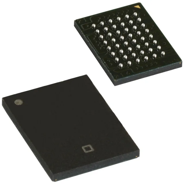
16 Mbit asynchronous SRAM in a 48-ball BGA
The CY7C1061GE30-10BV1XI: The parallel interface is a straightforward address/data bus with no refresh overhead, which simplifies the memory controller logic in FPGAs or ASICs.
For a processor or FPGA running a 50 MHz bus (20 ns period), the memory has half a clock cycle to respond before the host latches the data. That leaves margin for PCB trace delay and signal-integrity settling, but a 66 MHz bus (15 ns period) would require a faster part or a pipelined SRAM.
Package and layout: 48-VFBGA (6x8 mm)
The 48-VFBGA (6x8 mm) package uses a fine-pitch ball grid array. The tray shipping medium is standard for BGA parts and works with pick-and-place feeders that handle tray-fed components.