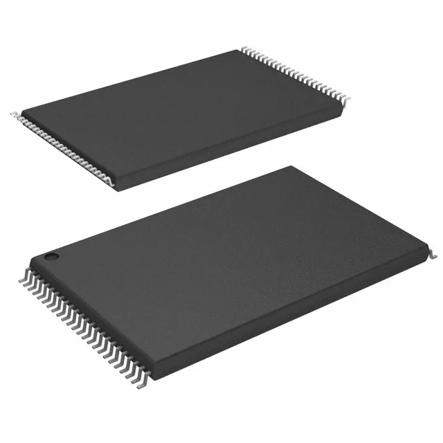
16Mbit asynchronous SRAM for 1.8V core logic buses
This part is typically used as a fast scratchpad or data buffer in networking equipment, base stations, industrial controllers, and test instrumentation where a parallel memory interface and low-voltage 1.8V logic are standard.
15 ns access time — timing margin on a 1.8V bus
At 1.8V, bus timing is tighter than at 3.3V; a 15 ns part gives comfortable margin for most 50-66 MHz ASIC or FPGA interfaces that expect a 20 ns or faster memory cycle.
The 1.65V to 2.2V supply covers the 1.8V nominal rail with headroom for ripple and drop — no external level translator needed when the host also runs at 1.8V. The 48-TSOP I footprint is a standard asynchronous SRAM pinout, so layout reuse across density upgrades is straightforward.