That access time is the spec that determines whether the memory can keep up with the bus controller without wait states — at 66 MHz a 15 ns window gives about one clock cycle of margin for address decode and data setup. At 100 MHz you are into the timing closure budget and may need to account for board trace delay. The 15 ns write cycle time matches the read access, so back-to-back transactions run at the same rate.
1.65 V to 2.2 V supply — low-voltage design fit
This SRAM runs from a 1.65 V to 2.2 V supply, which places it in the low-voltage memory tier for 1.8 V nominal core-logic designs. The 1.8 V domain also means lower dynamic power per access compared to 3.3 V asynchronous SRAMs of the same density.
Cypress (now Infineon) has announced the end of production; the final purchase window has passed or is closing. New- and surplus-stock through independent distribution is the remaining supply channel. If this SRAM is on your BOM, the procurement decision is about securing the remaining inventory before it dries up, or qualifying a pin-compatible alternative for long-term production.
54-TSOP II package — footprint and rework
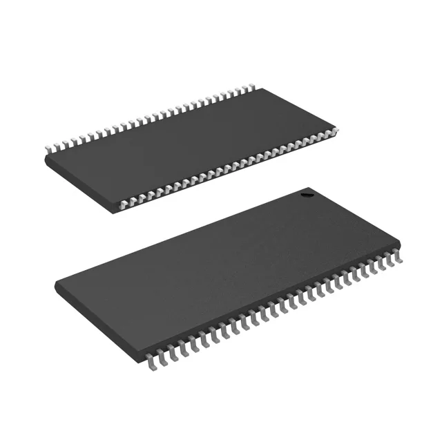
The 54-TSOP II (0.400", 10.16 mm width) is a standard JEDEC thin small-outline package for high-density memories. Surface-mount only — no socket option. If the board needs rework, a hot-air station with a fine nozzle and a preheat plate is the usual approach; the 0.5 mm lead pitch demands careful alignment during hand placement.