15 ns access — bus timing margin for the memory controller
The CY7C1061GE18-15BVXIT is a 16 Mbit asynchronous SRAM organized 1M x 16, with a 15 ns access time that sets the window for the memory controller to latch data after the address is valid. At a 66 MHz bus clock (15 ns period), the access time consumes the entire cycle — the controller must pipeline addresses or use a slower bus speed to maintain margin. The 15 ns write cycle time (word/page) matches the read access, so mixed read-write sequences don't introduce an asymmetry penalty.
1.65 V to 2.2 V supply — low-voltage core rail fit
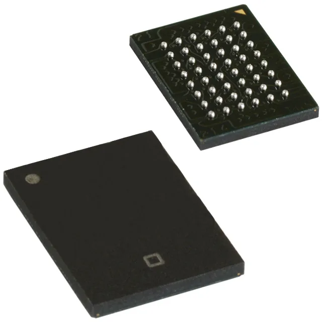
Operating from 1.65 V to 2.2 V, this SRAM mates directly with 1.8 V nominal logic cores without a level translator on the address and data buses. The 1.65 V minimum covers the low end of a 1.8 V rail under load, while the 2.2 V maximum allows a small boost margin for noise. The 48-VFBGA (6x8) package with 0.5 mm ball pitch demands a 4-layer PCB for fan-out — the inner layers carry the supply and ground planes that keep the VDD bounce under 5 % during simultaneous switching of all 16 data lines.
The 15 ns access time is specified across the full temperature range — no speed derating at the hot end, so the bus timing budget holds steady in a 70°C cabinet on a summer afternoon.
Active lifecycle — no imminent EOL
Infineon lists the CY7C1061GE18-15BVXIT as Active. Tape & Reel packaging means it feeds directly into a pick-and-place line — store the reels in a dry cabinet below 30°C / 60 % RH to keep the VFBGA moisture sensitivity level (MSL) within the floor-life rating.