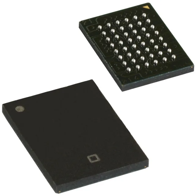
16 Mbit asynchronous SRAM in a 48-ball BGA
The CY7C1061GE18-15BV1XI is a 16 Mbit asynchronous SRAM organized as 1M x 16 bits, accessed through a parallel interface with a 15 ns access time. The 1.65 V to 2.2 V supply rail places it in the low-voltage SRAM class, drawing less dynamic power than a 3.3 V part at the same bus speed. The 48-VFBGA (6x8 mm) package demands a 4-layer PCB minimum for signal fan-out from the 0.5 mm ball pitch. Asynchronous SRAM requires no refresh clock or address multiplexing — the controller drives the address bus and strobes chip enable and output enable to read or write. The 15 ns access time gives the memory controller a 66 MHz theoretical ceiling for back-to-back reads, though board trace delay and capacitive loading on the parallel bus will reduce the practical margin.
Industrial temperature and supply voltage range
The 1.65 V to 2.2 V supply range aligns with 1.8 V logic families — the I/O levels are compatible with a 1.8 V FPGA or SoC bank without external level shifters. The 15 ns write cycle time applies to both word and page-mode writes. Page-mode writes let the controller burst up to four words at the same address row, reducing the per-word cycle overhead during cache-line fills or FIFO buffer updates.