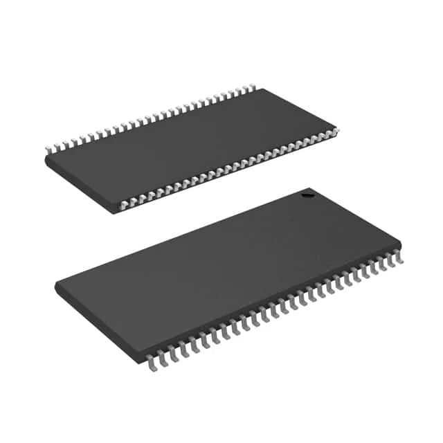
10 ns asynchronous SRAM — bus timing and memory sizing
This part is typically used in networking equipment, industrial controllers, and test instrumentation where fast, deterministic read/write cycles are needed on a legacy 5V bus.
10 ns access time — timing margin for the memory bus
For a system clocked at 100 MHz, that leaves roughly 10 ns of setup margin before the next clock edge — enough for a single-cycle read if the controller's output hold and trace delay are managed.
1M x 16 organization — bus width match
The 1M x 16 organization means the part presents a 16-bit data bus. If your processor or FPGA memory controller expects a 16-bit word, this is a direct fit. For a 32-bit bus you need two devices in parallel, with the address and control lines shared and the chip selects gated by the upper address bits.
Industrial temperature range and 5V supply
If you are on a 3.3V bus, look at the CY7C1061G33 series instead.
Housed in a 54-TSOP II (0.400" body width, 10.16 mm), this is a surface-mount package with JEDEC-standard footprint. The 0.8 mm pin pitch is fine for hand assembly but benefits from a stencil and reflow profile.
Listed as Active with no last-time-buy notice. That means Infineon is still manufacturing this part, and the normal supply chain is open.