10 ns access time — what it means for the bus cycle
CY7C1061GE-10BVXI is a 16 Mbit asynchronous SRAM organized as 1M x 16. The 10 ns access time is the max delay from address valid to data valid on the bus — the host processor must stretch its read cycle or insert wait states if its memory controller clock period is shorter than this window. No refresh or latency penalty — the asynchronous interface lets the memory sit in a simple memory-mapped address space without a controller state machine.
This rules out 3.3 V-only systems without a regulator — the part draws its full operating current from the 5 V rail, and the input thresholds are TTL-compatible at that level.
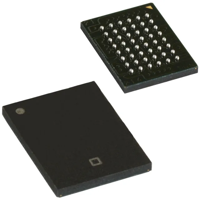
Package — 48-VFBGA (6x8 mm)
Supplied in a 48-ball VFBGA, 6x8 mm body. The fine-pitch BGA demands a controlled reflow profile — no hand-solder, no hot-air rework without a bottom-side preheat. The supplier device package is the same 48-VFBGA (6x8), so the footprint is standard across the CY7C1061 family.