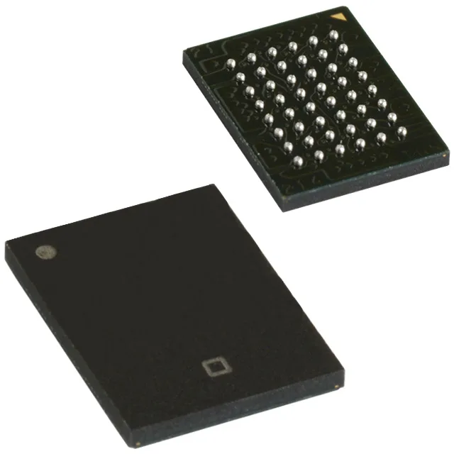
The CY7C1061GE-10BVJXIT: This part is intended for high-speed cache, buffer, and scratchpad memory in systems where deterministic, cycle-by-cycle read/write access is required — think networking equipment, industrial controllers, test instrumentation, and legacy DSP farms that still run on a 5 V bus.
10 ns access — timing margin and bus fit
The 10 ns access time and 10 ns write cycle time are the headline numbers here. For a 16 Mbit asynchronous SRAM, 10 ns is in the fast tier — most density-equivalent parts from the same era run 12 ns or 15 ns. That 2 ns to 5 ns margin matters when the memory is on a shared bus with a fast CPLD or FPGA controller: it gives the address decode logic more slack before the data must be valid. The 1M x 16 organization is a 16-bit-wide data path, so a single chip serves a 16-bit microcontroller or a 32-bit processor in a 16-bit boot mode without external byte-lane muxing. The parallel interface is straightforward to route — no clock, no strobe sequencing — but the 48-VFBGA (6x8 mm) package demands a fine-pitch BGA layout with micro-vias or blind vias if the board is multilayer.
It is not a 3.3 V part, so if your system runs on 3.3 V logic, you need a level translator or a separate 5 V regulator for the memory bank. The 48-VFBGA package with a 6x8 mm body is a space-saver — roughly 25% smaller than a 44-pin TSOP II footprint — but the 0.5 mm or 0.65 mm ball pitch means the PCB fab needs at least a Class 3 capability for reliable solder joints.
That means no looming LTB risk for a production BOM. For dual-sourcing resilience, the base product number CY7C1061 covers multiple speed and package variants — the -10BVJXIT suffix denotes the 10 ns speed grade, the 48-VFBGA package, and the Tape & Reel carrier. If your layout can accommodate a 44-pin TSOP II, the CY7C1061 family includes that option, but the BGA variant is the one you have here.