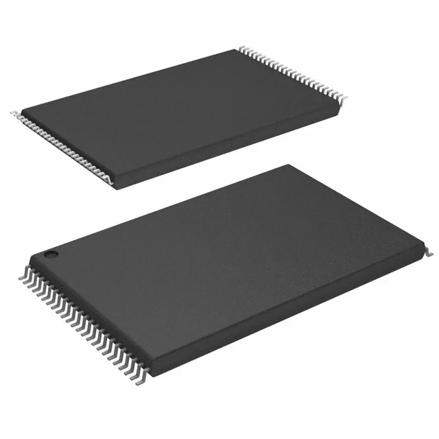
Infineon Technologies CY7C1061G30-10ZXET — Memory (DRAM / SRAM / Flash / EEPROM)

Infineon CY7C1061G30-10ZXET Async SRAM, 16Mbit, 10 ns

MPNCY7C1061G30-10ZXET
End of Life

Infineon Technologies CY7C1061G30-10ZXET, asynchronous SRAM, 16Mbit (1M x 16), 10 ns access time, 2.2V-3.6V supply, 48-TSOP I, Tape & Reel, -40°C to 85°C.

$35.7500Ref. price · indicative, final on quote
Independent supplier — new & surplus stockAuthenticity-screened · ESD-safe packingListing updated Aug 2026

Specifications

CY7C1061G30-10ZXET specifications
ParameterValue
Memory typeVolatile
MountingSurface Mount
Supply voltage2.2V ~ 3.6V
Memory interfaceParallel
Operating temperature-40°C ~ 85°C (TA)
PackageTape & Reel (TR)
TechnologySRAM - Asynchronous
Access time10 ns
Memory size16Mbit
Memory formatSRAM
Case48-TFSOP (0.724\", 18.40mm Width)
Memory organization1M x 16
Write cycle time - word, page10ns

Product details

16-Mbit asynchronous SRAM in a 48-TSOP I footprint

The Infineon CY7C1061G30-10ZXET is a 16 Mbit asynchronous SRAM organized 1M x 16, with a 10 ns access time that sets the bus cycle ceiling for the memory controller. Housed in a 48-TSOP I (0.724" body width), this surface-mount package routes 48 pins on a 0.50 mm pitch — the same footprint as the industry-standard TSOP I pinout, so it drops onto existing board layouts without a spin.

Frequently asked questions

What is the memory organization of the CY7C1061G30-10ZXET?

It is organized as 1M words by 16 bits (1M x 16), giving a total of 16 Mbit of storage. The 16-bit-wide data bus matches processors and FPGAs with a 16-bit external memory interface without needing byte-lane muxing.

What is the access time and write cycle time for this SRAM?

The access time is 10 ns, and the write cycle time (word, page mode) is also 10 ns. This means the memory can complete a read or write operation every 10 ns, corresponding to a 100 MHz bus cycle if the controller can sustain back-to-back accesses without wait states.