It operates from a 2.2V to 3.6V supply, covering both 2.5V and 3.3V logic rails without a separate regulator.
Memory organization and bus width
The 1M x 16 organization provides a 16-bit wide data bus, which matches 16-bit microcontrollers and DSPs without needing byte-lane muxing. The parallel interface uses standard chip-enable, output-enable, and write-enable signals, so timing integration is straightforward with most memory controllers. The write cycle time matches the read access time at 10 ns, allowing symmetric read/write throughput.
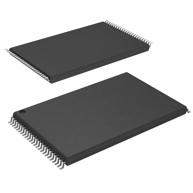
Housed in a 48-TFSOP (0.724" body width, 18.40 mm), the part uses the industry-standard 48-pin TSOP I footprint. This package is shared across many asynchronous SRAMs in the 8 Mbit to 32 Mbit range, so a layout designed for this part can often accommodate a second-source or density upgrade without a board spin.