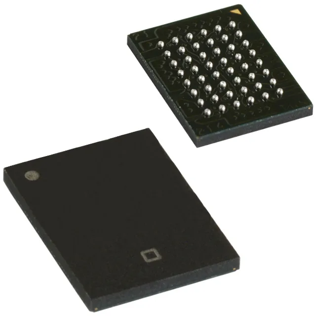
15 ns asynchronous SRAM for industrial memory maps
The Cypress (Infineon) CY7C1061G18-15BVJXI is a 16 Mbit asynchronous SRAM organized 1M × 16, delivering a 15 ns access time that sets the bus-turnaround floor for a parallel memory interface. Running from a 1.65 V to 2.2 V core supply, it targets low-voltage designs where a 3.3 V I/O bank is not available or where the memory bus shares a 1.8 V rail with the SoC. The 48-VFBGA (6×8 mm) package keeps the footprint compact, but the BGA pitch demands careful PCB escape routing and a controlled reflow profile.
Access time and bus timing
The 15 ns access time governs the address-to-data valid window. In a system with a 66 MHz bus clock (15 ns period), this part leaves almost no margin for address propagation delay and setup time — the bus controller must be rated for zero-wait-state operation at that speed. At 50 MHz (20 ns period) there is roughly 5 ns of margin for PCB trace delay and logic propagation, which is workable with careful layout.
The 1.65 V minimum supply helps maintain data retention during a brown-out event common in 1.8 V core domains. The 48-VFBGA package is a fine-pitch BGA (0.5 mm ball pitch typical for the 6×8 mm array) — the board finish needs to be OSP or ENIG, and the reflow profile must follow the JEDEC MSL rating of the device (typically MSL 3).
The base product number CY7C1061 covers multiple speed and package variants — the -15BVJXI suffix identifies the 15 ns, 48-VFBGA, industrial-temperature version. For dual-sourcing, look at the same base number with the same speed and package code from the same manufacturer; no second-source alternate is listed on this record.