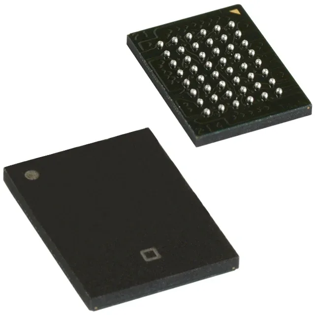
16 Mbit asynchronous SRAM — 10 ns access on a 5 V parallel bus
The CY7C1061G-10BVXI is a 16 Mbit asynchronous SRAM organized as 1M x 16, meaning it presents a full 16-bit word on each read cycle without byte-lane multiplexing — a natural fit for 16-bit microcontrollers and legacy DSP buses that expect a wide parallel memory interface. The 10 ns access time sets the read-cycle floor: at a 100 MHz bus clock the memory can return data within a single cycle, but the address-to-data valid window must be budgeted against the controller's setup time and the PCB trace delay on the 48-VFBGA fan-out.
That matters for a BOM that still carries 5 V peripherals or a legacy ASIC; a level translator is not needed on the address/data bus.
48-VFBGA package — board integration notes
Housed in a 48-ball VFBGA measuring 6 x 8 mm, the package uses a fine-pitch ball array — typically 0.75 mm pitch — which demands a 4-layer PCB for signal fan-out and a solid ground plane under the BGA to control crosstalk on the 16-bit data bus at 10 ns edge rates. Supplied in Tray packaging, the parts arrive in JEDEC-standard matrix trays suitable for pick-and-place without reel taping — confirm the feeder setup if the line expects tape-and-reel format.