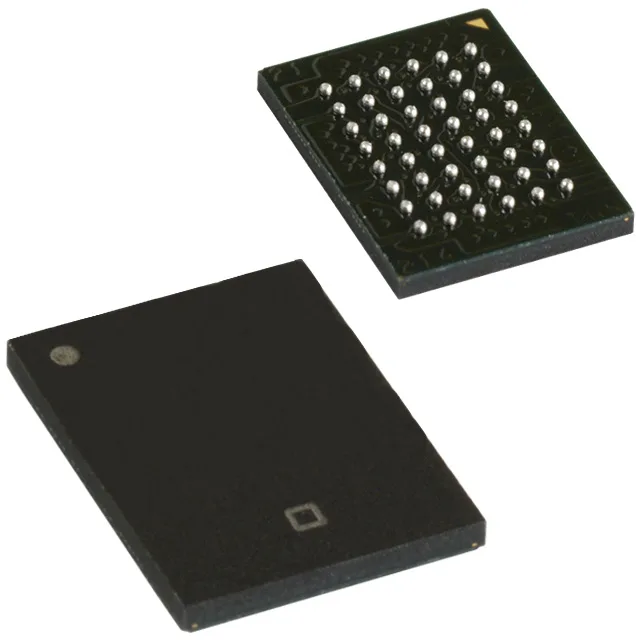
10 ns asynchronous SRAM for 5V cache and buffer applications
The 10 ns access time and 10 ns write cycle time mean the part can sustain back-to-back read or write operations at 100 MHz bus speed, provided the controller meets the setup/hold windows. The 1M x 16 organization maps directly to a 16-bit data bus, so no byte-lane steering logic is needed — the address bus increments per 16-bit word. For 8-bit controllers, the upper and lower bytes are accessed by toggling the byte-enable pins (UB/LB) on the same address, which the asynchronous interface handles without a clock.
Industrial temperature range and 48-ball VFBGA footprint
The 48-VFBGA (6x8 mm) package saves about 40% board area compared to a 44-pin TSOP, but the 0.5 mm ball pitch demands fine-line routing and a four-layer PCB with microvias if the controller is on the opposite side. The VFBGA's exposed center pad (thermal land) must be connected to a solid ground plane with at least nine thermal vias to keep junction temperature within limits at full bus activity. Decoupling with a 100 nF ceramic per supply pin pair, placed within 2 mm of the balls, is the standard layout practice for 10 ns edge rates.