Infineon Technologies CY7C1061G-10BV1XI — Memory (DRAM / SRAM / Flash / EEPROM)

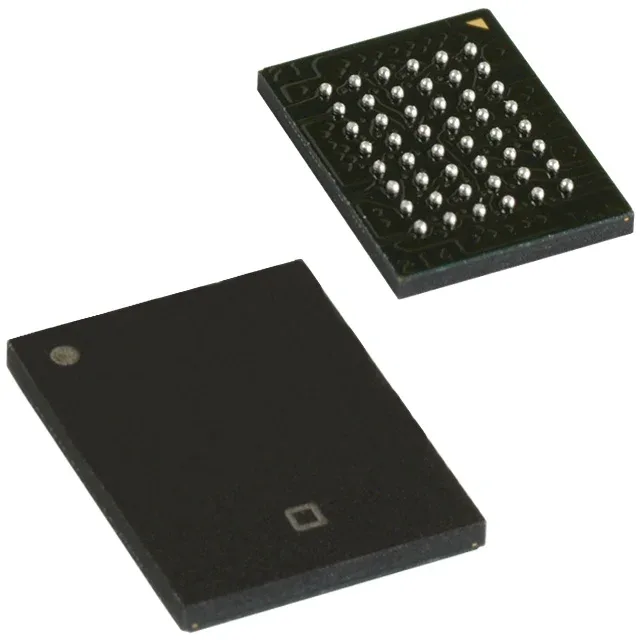
CY7C1061G-10BV1XI Infineon 16Mbit Async SRAM, 10ns, 48-VFBGA

MPNCY7C1061G-10BV1XI
Active

Infineon Technologies CY7C1061G-10BV1XI asynchronous parallel SRAM, 16Mbit (1M x 16), 10 ns access time, 4.5–5.5 V supply, 48-VFBGA (6x8 mm), -40 to 85 °C, tray.

$38.5000Ref. price · indicative, final on quote
Independent supplier — new & surplus stockAuthenticity-screened · ESD-safe packingListing updated Aug 2026

Specifications

CY7C1061G-10BV1XI specifications
ParameterValue
Memory typeVolatile
MountingSurface Mount
Supply voltage4.5V ~ 5.5V
Memory interfaceParallel
Operating temperature-40°C~85°C(TA)
PackageTray
TechnologySRAM - Asynchronous
Access time10 ns
Memory size16Mbit
Memory formatSRAM
Case48-VFBGA
Memory organization1M x 16
Write cycle time - word, page10ns

Product details

16Mbit asynchronous SRAM — 10 ns access, 5 V I/O

The CY7C1061G-10BV1XI: The 10 ns access time means the part can deliver data within one 100 MHz clock cycle from address assertion — the limiting factor in a fast bus is the address-to-data propagation, not the memory itself.

Industrial temperature grade and board integration

The 48-VFBGA (6x8 mm) package is a fine-pitch BGA — the 0.5 mm ball pitch demands a controlled impedance PCB stack-up with micro-vias for fan-out; a two-layer board won't route the inner rows. The 1M x 16 organization gives a 16-bit data bus in a single package — a 32-bit memory word needs two devices, but the 16-bit width halves the chip count versus an 8-bit wide part for the same density.

Active lifecycle — sourcing posture

The base product number CY7C1061 covers multiple speed grades and package variants — the -10BV1XI suffix locks in the 10 ns access, 48-VFBGA, and industrial temperature range.

Frequently asked questions

What does the 10 ns access time mean for my bus timing?

The 10 ns access time is the maximum delay from address valid to data valid on the bus — a 100 MHz controller can read the SRAM in a single clock cycle without wait states, provided the address setup and hold margins are met.

What package does CY7C1061G-10BV1XI use?

48-VFBGA (6x8 mm) — a fine-pitch BGA with 0.5 mm ball pitch. Requires a multi-layer PCB with micro-vias for signal breakout.