That 10 ns figure is the time from address change to valid data on the outputs — it sets the minimum bus cycle time when the memory is used without wait states. For a 16-bit data bus running at 66 MHz (15 ns period), a 10 ns access leaves 5 ns of setup margin to the controller's data latch. At 100 MHz (10 ns period), the margin disappears and the controller must insert a wait state or use a synchronous SRAM instead.
Package and footprint — 54-TSOP II
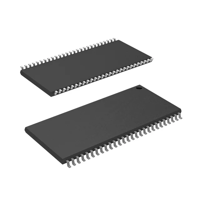
The part comes in a 54-TSOP II package (0.400" body width, 10.16 mm), surface-mount. The TSOP II footprint is a standard JEDEC outline shared across many 16 Mbit asynchronous SRAMs from multiple vendors, so the PCB layout is portable if a second source is needed later. The supplier device package is 54-TSOP II — the same as the package / case field, just the Infineon naming.