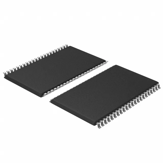
Infineon Technologies CY7C1059DV33-12ZSXQT — Memory (DRAM / SRAM / Flash / EEPROM)

Infineon CY7C1059DV33-12ZSXQT SRAM, 8Mbit, 12 ns, 44-TSOP II

MPNCY7C1059DV33-12ZSXQT
Obsolete

Infineon CY7C1059DV33-12ZSXQT, 8Mbit asynchronous SRAM, 1M x 8 organization, 12 ns access time, parallel interface, 3V–3.6V supply, -40°C to 85°C, 44-TSOP II, Tape & Reel.

$11.7000Ref. price · indicative, final on quote
Independent supplier — new & surplus stockAuthenticity-screened · ESD-safe packingListing updated Jul 2026

Specifications

CY7C1059DV33-12ZSXQT specifications
ParameterValue
Memory typeVolatile
MountingSurface Mount
Supply voltage3V ~ 3.6V
Memory interfaceParallel
Operating temperature-40°C ~ 85°C (TA)
PackageTape & Reel (TR)
TechnologySRAM - Asynchronous
Access time12 ns
Memory size8Mbit
Memory formatSRAM
Case44-TSOP (0.400\", 10.16mm Width)
Memory organization1M x 8
Write cycle time - word, page12ns

Product details

The Infineon CY7C1059DV33-12ZSXQT is an 8Mbit asynchronous SRAM organized as 1M x 8, with a 12 ns access time and a parallel interface. It operates from a 3V to 3.6V supply and is rated for -40°C to 85°C.

A 12 ns access time means the SRAM presents valid data on the data bus within 12 ns of the address being latched.

Obsolete — sourcing reality for this SRAM

Frequently asked questions

What is the replacement for CY7C1059DV33-12ZSXQT?

No official replacement order code is listed by Infineon. For new designs, evaluate current-production asynchronous SRAMs in 44-TSOP II from ISSI, Alliance Memory, or Renesas — verify pin-compatibility against your layout.

Is CY7C1059DV33-12ZSXQT compatible with 3.3V?

Yes, the supply voltage range is 3V to 3.6V, making it directly compatible with a 3.3V logic rail.

What is the pinout of CY7C1059DV33-12ZSXQT?

The pinout follows the standard 44-TSOP II footprint for a 1M x 8 asynchronous SRAM. The datasheet (available on request) provides the full pin assignment and timing diagrams.