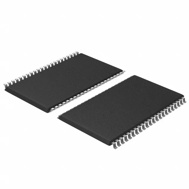
Infineon Technologies CY7C1059DV33-12ZSXIT — Memory (DRAM / SRAM / Flash / EEPROM)

Infineon CY7C1059DV33-12ZSXIT SRAM, 12 ns, 8 Mbit, 44-TSOP II

MPNCY7C1059DV33-12ZSXIT
End of Life

Infineon CY7C1059DV33-12ZSXIT, asynchronous SRAM, 8 Mbit (1M x 8), 12 ns access time, parallel interface, 3V to 3.6V supply, -40°C to 85°C, 44-TSOP II, Tape & Reel.

Independent supplier — new & surplus stockAuthenticity-screened · ESD-safe packingListing updated Aug 2026

Specifications

CY7C1059DV33-12ZSXIT specifications
ParameterValue
Memory typeVolatile
MountingSurface Mount
Supply voltage3V ~ 3.6V
Memory interfaceParallel
Operating temperature-40°C ~ 85°C (TA)
PackageTape & Reel (TR)
TechnologySRAM - Asynchronous
Access time12 ns
Memory size8Mbit
Memory formatSRAM
Case44-TSOP (0.400\", 10.16mm Width)
Memory organization1M x 8
Write cycle time - word, page12ns

Product details

12 ns access time — what it means for the bus

The 12 ns access time sets the window from address valid to data valid on a read cycle. The write cycle time matches at 12 ns, so back-to-back writes at the same speed are possible.

Lifecycle and sourcing

The CY7C1059DV33-12ZSXIT is listed with an EOL lifecycle stage. This means the part is in its last-time-buy or phase-out window. No official successor is recorded. For BOM lines that require this exact density and speed grade, sourcing is through independent distribution — quoted to order against an RFQ, with availability and current pricing confirmed at quote time.

Frequently asked questions

Is CY7C1059DV33-12ZSXIT obsolete?

The CY7C1059DV33-12ZSXIT is listed with an EOL lifecycle stage, indicating it is in a phase-out or last-time-buy window.

What is the access time of CY7C1059DV33-12ZSXIT?

The access time is 12 ns for both read and write cycles.

What voltage does CY7C1059DV33-12ZSXIT require?

The supply voltage range is 3V to 3.6V.