For a system architect clocking a 100 MHz memory controller, that leaves roughly 5 ns of setup margin after accounting for PCB trace delay and clock jitter — enough to avoid adding a second wait state. The 512K x 16 organization gives a 16-bit data path per chip, so two devices can build a 32-bit memory bank without external muxing.
For the storeroom keeper planning a five-year service spares budget, this part does not need a panic stock-up now.
Package and footprint — 44-TSOP II
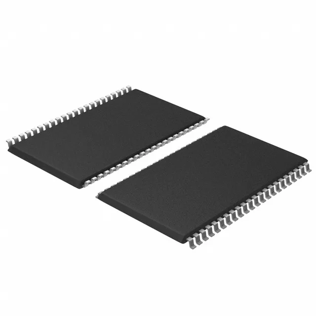
Housed in a 44-TSOP II (0.400" body width, 10.16 mm wide), this is a surface-mount package with a 0.8 mm lead pitch. The footprint matches the standard JEDEC TSOP II layout, so it drops onto a board that already carries a 44-pin TSOP II SRAM. The supplier device package is explicitly 44-TSOP II — confirm the orientation notch before placement; the pin-1 indicator is on the top-left corner when the notch faces left.