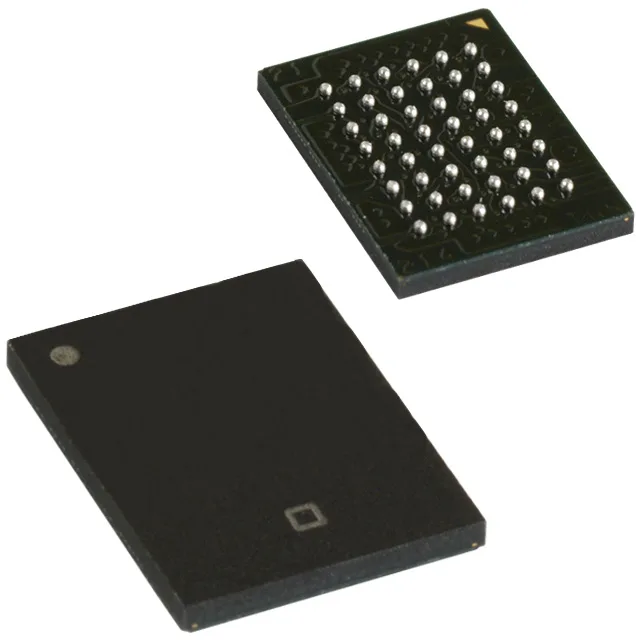
For a system clocked at 100 MHz (10 ns period), that leaves zero margin for address-to-data in a single cycle — the designer typically runs the memory on a divided clock or uses a registered read to capture the data. On a 66 MHz bus (15 ns period), the 10 ns access gives a comfortable 5 ns of setup margin before the latching edge. The write-cycle time is also 10 ns, so back-to-back writes at 100 MHz are possible if the write pulse is timed correctly.
The supply range of 2.2V to 3.6V means it can work in a system that drops to 2.5V or 2.2V during battery discharge, as long as the core logic is compatible. Surface-mount only — no through-hole option.