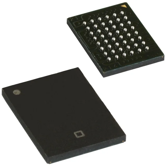
10 ns asynchronous SRAM for industrial and embedded systems
The 48-ball VFBGA (6x8 mm) footprint saves board area compared to TSOP alternatives, though the fine 0.75 mm pitch demands careful PCB routing and a solder stencil matched to the land pattern.
For a processor running at 50 MHz (20 ns cycle), this leaves a 10 ns window for address decode, board trace delay, and setup time at the CPU — tight but achievable with proper layout. At 66 MHz (15 ns cycle), the margin shrinks to 5 ns, which may force a faster part or a pipelined memory controller. The write cycle time matches the read at 10 ns, so back-to-back operations hit the same throughput without dead cycles.
Package and rework realities for the 48-VFBGA
The 48-VFBGA (6x8 mm) with 0.75 mm ball pitch is a fine-pitch BGA that requires a solder paste stencil with 0.35 mm apertures and a reflow profile peaking at 245°C peak (SnAgCu). MSL 3 out of the bag — if the moisture barrier pouch has been open longer than 168 hours, bake at 125°C for 48 hours before reflow. X-ray inspection after soldering catches head-in-pillow and voiding above 25% area per ball. For rework, a bottom-side preheat at 150°C and a hot-air nozzle matching the 6x8 mm body works; the adjacent passive components need shielding from the airflow.
The base product number CY7C1051 covers multiple speed and temperature variants in the same 48-VFBGA footprint, so a speed upgrade (e.g., 8 ns) or wider temperature range is a drop-in swap if needed. For dual-sourcing resilience, the asynchronous 512K x 16 SRAM market has several pin-compatible offerings from other manufacturers — verify the supply voltage and temperature grade match before substituting.