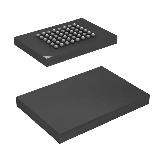
The 48-TFBGA package (6x8 mm body) keeps the footprint compact, but the fine-pitch BGA demands careful PCB layout — via-in-pad or microvia fanout is typical for routing the 16-bit data bus and address lines.
For a processor running a 100 MHz bus (10 ns cycle), this SRAM can deliver data in a single cycle if the controller's address-to-data setup requirement is met — no wait-state insertion needed. If your system clock is faster than 100 MHz, you'll need to evaluate the combined timing of address hold, output enable, and chip select against the processor's memory controller specs; a 10 ns part at 133 MHz (7.5 ns cycle) typically requires one wait state.
Package and footprint — 48-TFBGA (6x8 mm)
The fine pitch means the PCB needs at least four layers for fanout — two signal layers for the address/data bus plus power and ground planes. Decoupling capacitors should sit as close to the BGA footprint as possible, ideally on the opposite side of the board under the package, with multiple vias to the power plane. The package is surface-mount only; no socket option exists for this footprint.