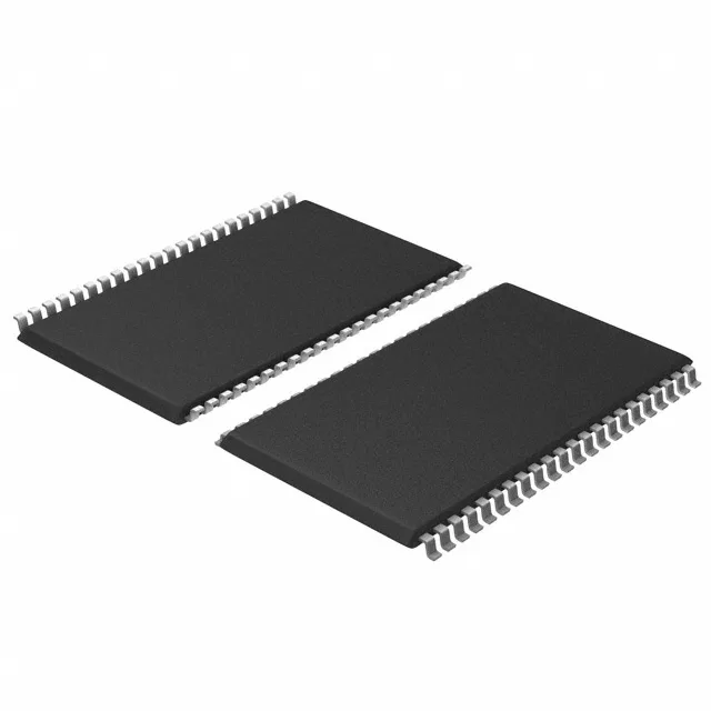
10 ns asynchronous SRAM — 4 Mbit in a 44-TSOP II
The CY7C1049GN30-10ZSXI: The part comes in a 44-pin TSOP II (thin small-outline package) for surface-mount assembly. This is a volatile memory — data is retained only while power is applied.
This part is active with no last-time-buy notice. The base product number CY7C1049 covers multiple speed and temperature grades — if your design can tolerate a slower access time or a wider temperature range, there are pin-compatible siblings in the same family.
Package and footprint — 44-TSOP II, tray delivery
The 44-TSOP II package (0.400-inch body width, 10.16 mm) is a standard JEDEC outline for asynchronous SRAMs in this density range. It is a surface-mount package with gull-wing leads on 0.8 mm pitch. The part ships in a tray, not tape-and-reel — factor that into your pick-and-place feeder setup if you are running high-volume assembly; you will need a tray feeder or a tube-to-tape conversion step. The tray is an anti-static, stackable carrier that protects the leads during storage and handling. For reflow, the MSL rating (not stated in this record but typical for TSOP-II SRAMs from Cypress) is MSL 3 — so if the moisture-barrier bag has been open longer than 168 hours, bake the trays at 125°C for 48 hours before reflow to avoid popcorning.
Memory organisation and interface — parallel bus, byte-wide access
The 512K x 8 organisation means the part presents an 8-bit data bus with 19 address lines (A0–A18). It uses a standard asynchronous parallel interface: chip enable (CE), output enable (OE), and write enable (WE) control the bus. For a microcontroller with an external bus interface (e.g., an STM32F7 or an i.MX RT in FlexBus mode), this SRAM can be mapped directly into the memory space with no glue logic. The byte-wide organisation is convenient for 8-bit microcontrollers or for storing 8-bit data words; for a 16-bit or 32-bit bus, you would use two or four of these in parallel with shared address lines.