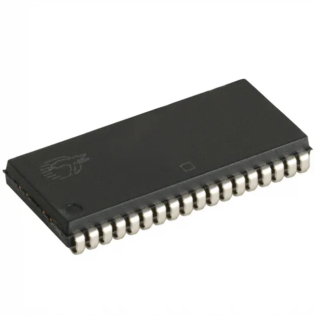
What this async SRAM does in a system
This part is used as a fast scratchpad, cache buffer, or working memory in embedded systems where deterministic access latency matters more than the density of a DRAM or the endurance limits of a Flash. It comes in a 36-SOJ surface-mount package, a legacy but still widely supported footprint for through-hole-alternative SRAM on multilayer boards.
10 ns access time — timing budget for the bus
The 10 ns access time and equal 10 ns write cycle time are the headline ratings for this SRAM. For a system architect, that 10 ns window defines how much of the bus cycle is consumed by the memory itself. With a 100 MHz bus clock (10 ns period), the SRAM consumes the entire cycle if the controller's address-to-output propagation is tight. In practice, a 66 MHz or 80 MHz bus leaves enough margin for PCB trace delays and output hold. The 512K x 8 organization means byte-wide access — useful for 8-bit MCUs or as a data buffer in a 32-bit system where four chips are banked. The parallel interface is straightforward to wire, but the 36-SOJ footprint needs a land pattern that matches the 0.400-inch body width.
No PCN bulletins have flagged this specific order code for end-of-life. The base product number CY7C1049 covers the whole family, so if a different speed or package variant is needed later, the same design rules apply.