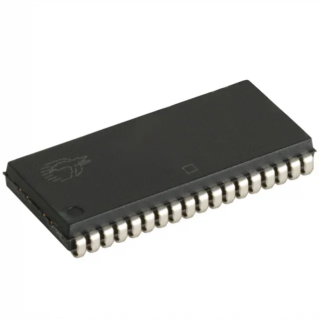
Infineon Technologies CY7C1049GN-10VXIT — Memory (DRAM / SRAM / Flash / EEPROM)

Infineon CY7C1049GN-10VXIT 4Mbit Async SRAM, 10 ns, 5 V

MPNCY7C1049GN-10VXIT
Active

Infineon CY7C1049GN-10VXIT, 4Mbit asynchronous SRAM, 512K x 8 organization, 10 ns access time, parallel interface, 4.5 V to 5.5 V supply, -40°C to 85°C, 36-SOJ package, Tape & Reel.

$7.0800Ref. price · indicative, final on quote
Packaging36-BSOJ (0.400", 10.16mm Width)
RoHSROHS3 Compliant
Independent supplier — new & surplus stockAuthenticity-screened · ESD-safe packingListing updated Aug 2026

Specifications

CY7C1049GN-10VXIT specifications
ParameterValue
Memory typeVolatile
MountingSurface Mount
Supply voltage4.5V ~ 5.5V
Memory interfaceParallel
Operating temperature-40°C ~ 85°C (TA)
PackageTape & Reel (TR) Cut Tape (CT)
TechnologySRAM - Asynchronous
Access time10 ns
Memory size4Mbit
Memory formatSRAM
Case36-BSOJ (0.400\", 10.16mm Width)
Memory organization512K x 8
Write cycle time - word, page10ns

Product details

10 ns async SRAM for 5 V legacy buses

The 10 ns access time means it can service a 66 MHz bus without wait states — at 100 MHz you'd need to budget one wait state for back-to-back reads.

512K x 8 — byte-wide bus fit

The 512K x 8 organization is a straight byte-wide memory, ideal for 8-bit microcontrollers (8051, PIC, AVR) or as a data buffer in 8-bit mode on a 16/32-bit bus. If your design needs 16-bit word access, you would pair two of these or look at the 256K x 16 sibling CY7C1041G-10ZSXIT. The parallel interface is straightforward — address, data, chip enable, output enable, write enable — no clocked handshake, no refresh cycle to manage.

36-SOJ package — reflow and footprint notes

The 36-SOJ package (36-pin Small Outline J-lead, 10.16 mm body width) is a surface-mount form factor with J-bend leads tucked under the body. The J-bend also makes visual inspection of the solder joint harder; if your AOI system is set up for gull-wing only, you may need to adjust the inspection algorithm or add an X-ray spot-check.

It is ROHS3 compliant. For dual-sourcing flexibility, the CY7C1049G30-10VXIT is a functional equivalent with the same 4 Mbit density and 10 ns access time, but operates at 2.2 V supply — verify your 5 V rail can tolerate the lower voltage before substituting.

Frequently asked questions

What is the access time of CY7C1049GN-10VXIT?

The access time is 10 ns for both read and write cycles. This allows zero-wait-state operation on a 66 MHz bus and one wait state at 100 MHz.

What is the difference between CY7C1049GN-10VXIT and CY7C1049GN-10VXI?

The die, memory organization, speed, and temperature grade are identical.